Slide 1 of 5
Slide 1 - System Understanding
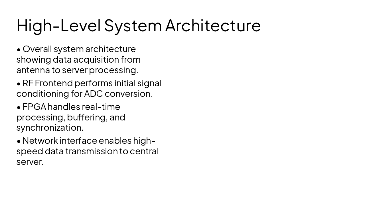
System Architecture and Signal Flow Overview
Ramp-Up Plan: System Understanding
---
Photo by Nastuh Abootalebi on Unsplash
Generated from prompt:
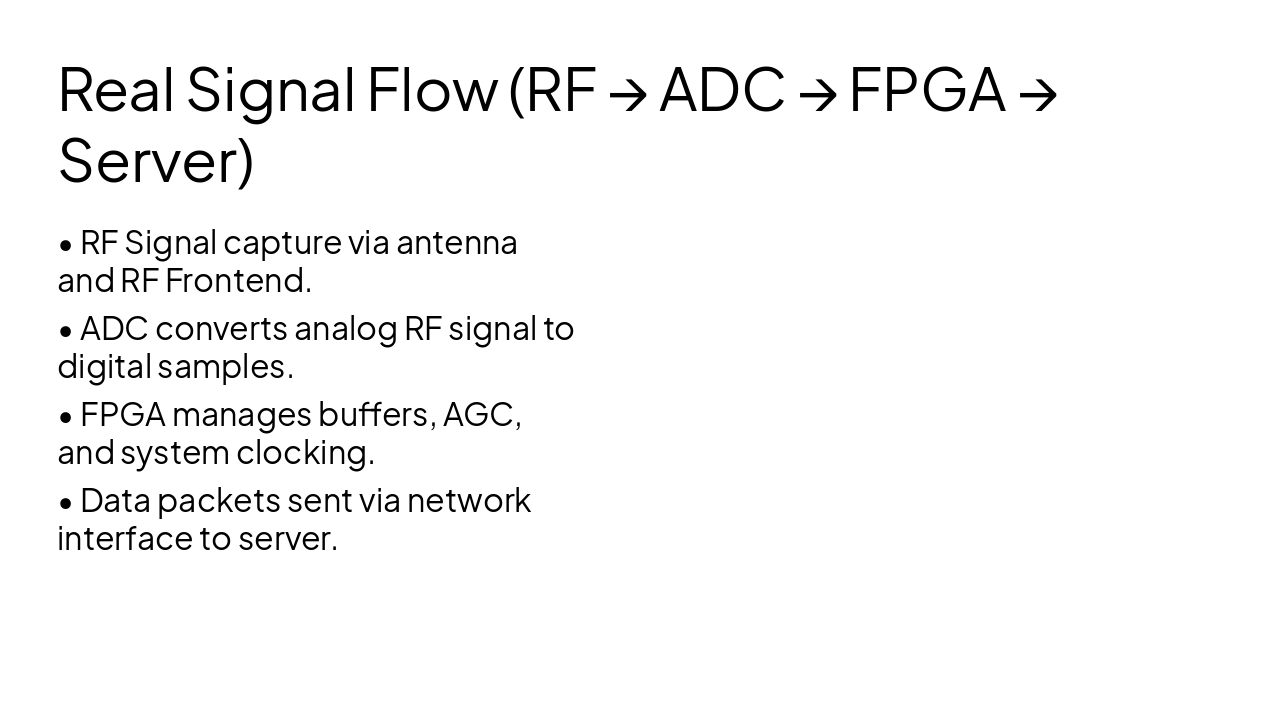
Update the existing presentation titled 'Ramp-Up Plan: System Understanding' to include a detailed real signal flow diagram. Add a new dedicated slide after the high-level architecture diagram: Slide Title: Real Signal Flow (RF → ADC → FPGA → Server) Content: - Visual end-to-end diagram showing: RF Signal (antenna) → RF Frontend → ADC → FPGA (with labeled internal blocks: sample buffers, AGC, clocking/sync, antenna control) → Network Interface → Server - Use arrows to clearly indicate direction of signal flow - Highlight data transformation stages (analog RF → digital samples → processed data → network packets) - Add small annotations for each stage (e.g., 'Analog RF capture', 'Digitization', 'Signal processing', 'Data transmission') Also enhance previous architecture diagram slide to align with this flow. Design: - Clean, modern, minimal text - Use icons for antenna, chip, server - Color-code stages (RF, digital, processing, network) - Make diagram the focal point of the slide Keep all previous slides intact and consistent.
This deck provides a comprehensive ramp-up on the RF signal processing system, covering high-level architecture, real-time signal flow from antenna to server, key transformation stages (RF frontend, ADC, FPGA), and next steps for integration and next
System Architecture and Signal Flow Overview
Ramp-Up Plan: System Understanding
---
Photo by Nastuh Abootalebi on Unsplash
End-to-End Signal Pipeline Successfully Implemented
Next steps in system integration and testing.
Explore thousands of AI-generated presentations for inspiration
Generate professional presentations in seconds with Karaf's AI. Customize this presentation or start from scratch.