Slide 1 - VLSI Technology
This title slide is titled "VLSI Technology." Its subtitle reads "Exam-Oriented Presentation with Diagrams & Answers."
VLSI Technology
Exam-Oriented Presentation with Diagrams & Answers
Source: ECE 3rd Year AKTU Syllabus

Generated from prompt:
Create a detailed presentation on 'VLSI Technology' for ECE 3rd Year (AKTU syllabus). Include full answers for a typical university paper: short answers for 2-mark questions and detailed explanations with diagrams for 7-mark questions. Cover the following topics comprehensively: 1. Introduction to VLSI Technology: definition, history, advantages, applications. 2. MOSFET fabrication process with detailed diagram. 3. Wafer preparation, oxidation, and diffusion. 4. Lithography process – optical and electron-beam lithography. 5. Ion implantation and metallization. 6. Packaging and testing. 7. CMOS technology and scaling. 8. Comparison between bipolar and CMOS technologies. 9. Recent trends in VLSI (FinFET, SOI, etc.). 10. Important topics per unit for AKTU syllabus (Unit 1–5). Make it concise yet exam-oriented, formatted clearly for presentation and PDF reading.
21-slide exam guide for AKTU ECE 3rd Yr VLSI: intro/history, MOSFET fab, wafer processes, lithography, implantation, CMOS scaling, bipolar vs CMOS, trends (FinFET/SOI), syllabus units w/ 2/7-mark answ
This title slide is titled "VLSI Technology." Its subtitle reads "Exam-Oriented Presentation with Diagrams & Answers."
Exam-Oriented Presentation with Diagrams & Answers
Source: ECE 3rd Year AKTU Syllabus

This agenda slide outlines a presentation on VLSI Technology with five key sections. It covers an introduction to VLSI, MOSFET fabrication processes, packaging/testing/CMOS scaling, comparisons/recent trends like FinFET/SOI, and AKTU syllabus units 1-5.
Definition, history, advantages, and applications.
Wafer prep, oxidation, diffusion, lithography, ion implant, metallization.
Packaging methods, testing procedures, CMOS technology, and scaling.
Bipolar vs CMOS, trends like FinFET, SOI.
Exam-oriented coverage of key topics.

This slide is a section header titled "1. Introduction to VLSI" (section 01). Its subtitle highlights the key topics: Definition, History, Advantages, and Applications.
01
Definition, History, Advantages & Applications
Source: AKTU ECE 3rd Year VLSI Technology Syllabus - Unit 1

The VLSI History Timeline slide highlights key milestones starting with the 1958 IC invention by Kilby and Noyce, followed by Intel's 1971 4004 microprocessor. It progresses through 1980s CMOS dominance, 1990s sub-micron fabrication, and 2000s+ nanoscale FinFET transistors.
1958: IC Invention by Kilby/Noyce Jack Kilby at TI and Robert Noyce at Fairchild invent the first integrated circuit. 1971: Intel 4004 First Microprocessor Intel releases the world's first commercial microprocessor, marking a milestone in VLSI. 1980s: CMOS Technology Dominance CMOS technology becomes dominant due to low power and high density advantages. 1990s: Sub-Micron Process Technology Fabrication advances to sub-micron scales, enabling higher integration levels. 2000s+: Nanoscale and FinFET Era Transition to nanoscale transistors, introduction of FinFET for better control.

This slide outlines key advantages of the technology, including miniaturization for compact devices, low power consumption, and high density with reliability. It also covers applications like microprocessors, ASICs, FPGAs, DSPs, AI chips, and enabling System-on-Chip (SoC) designs.
Source: VLSI Technology Presentation

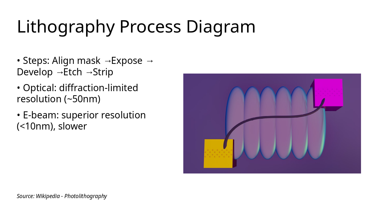
This slide serves as the section header for Section 2: MOSFET Fabrication Process. It lists the key nMOS/pMOS steps: Wafer Clean, Oxidize, Photoresist, Etch, Dope, and Metallize.
2.
nMOS/pMOS Steps: Wafer Clean, Oxidize, Photoresist, Etch, Dope, Metallize
Source: VLSI Technology - AKTU ECE 3rd Year

This slide diagrams the fabrication process for an n-channel MOSFET on a p-type silicon wafer substrate. It outlines seven steps: growing gate oxide, depositing and patterning the poly-Si gate, implanting n+ source/drain regions, forming sidewall spacers, silicidation with contact etching, and depositing metal interconnects.
Source: Wikipedia: MOSFET fabrication

This slide serves as the header for Section 3, titled "Wafer Preparation, Oxidation, Diffusion." It subtitles the key steps: Czochralski growth, slicing/polishing, dry/wet SiO2 oxidation, and high-temp dopant diffusion.
3
Czochralski growth, slicing/polishing, dry/wet SiO2 oxidation, high-temp dopant diffusion steps

This slide outlines the Deal-Grove model for linear/parabolic growth of thick oxides (>300Å), constant-source diffusion with erfc profiles, and limited-source diffusion with Gaussian profiles. It also covers Fick's laws (flux J=-D∇C and ∂C/∂t=D∇²C) plus sheet resistance calculations (Rs=ρ/t or 1/(qμ∫N(x)dx)).
Source: VLSI Technology - AKTU Syllabus

This section header slide in VLSI Technology introduces Section 04: Lithography Process. It contrasts optical lithography, using UV light and masks for photoresist, with maskless E-beam direct write for high resolution.
04
Optical: UV light & mask for photoresist; E-beam: maskless direct write for high resolution
Source: AKTU ECE 3rd Year Syllabus

The slide diagrams the lithography process with key steps: align mask, expose, develop, etch, and strip. It compares optical lithography's diffraction-limited resolution (~50nm) to e-beam lithography's superior resolution (<10nm), which is slower.
Source: Wikipedia - Photolithography

Ion implantation accelerates ions into a substrate, with dose controlling dopant concentration and energy determining depth/profile, followed by annealing to activate dopants and repair lattice damage. Metallization deposits Al or Cu films via sputtering, then patterns interconnects using lithography and etching.
Source: VLSI Technology - AKTU Syllabus

This slide features a diagram of the ion implantation process for doping silicon wafers. It outlines key steps: preparing the wafer, generating dopant ions in an ion source, accelerating them at high energy toward the wafer, and performing implantation followed by anneal activation.
Source: Ion implantation

This slide is a section header for Section 6: Packaging & Testing. It lists key processes like die attach, wire bond, encapsulation, and testing methods including wafer probe, functional, and burn-in.
6
Die attach, wire bond, encapsulation. Wafer probe, functional, burn-in testing.

Section 7 introduces "CMOS Technology & Scaling" as a section header slide. Its subtitle covers n/p transistors for low power, Dennard/Moore scaling, and limits from short channel effects.
07
n/p transistors for low power; Dennard/Moore scaling & short channel effects limits
Source: VLSI Technology - ECE 3rd Year (AKTU)

CMOS scaling classically uses constant field reduction of channel length (L), oxide thickness (tox), and Vdd, but faces limits from velocity saturation in short channels and leakage via subthreshold conduction and gate oxide tunneling. Solutions include high-k dielectrics for thinner EOT with lower leakage, and metal gates to eliminate poly depletion and improve control.
Source: AKTU VLSI Technology Syllabus

The slide compares Bipolar and CMOS technologies in a two-column format. Bipolar excels in high speed (ns switching) for analog/high-performance apps but suffers from high power dissipation, low density, and high cost, while CMOS offers low power (uW range), high density with scaling, low cost, moderate speed, and scalability for digital/VLSI.
| Bipolar | CMOS |
|---|
| High speed (ns switching) High power dissipation Low density High cost Analog/high-performance apps | Low power (uW range) High density (scaling) Low cost Moderate speed Digital/VLSI scalable |
Source: VLSI Technology - AKTU ECE 3rd Year

Recent VLSI trends highlight advanced transistors like FinFET for superior gate control, SOI to cut parasitic capacitance and leakage, and GAA for enhanced electrostatics. Additionally, 3D IC stacking boosts density while EUV lithography enables sub-7nm features.
Source: AKTU ECE 3rd Year Syllabus

This slide serves as the section header for Section 10, titled "AKTU Syllabus Units 1-5." The subtitle lists key topics: Intro/Fab, MOS/CMOS, Layout/Design, Testing, and Trends/Apps.
10
Intro/Fab, MOS/CMOS, Layout/Design, Testing, Trends/Apps
Source: AKTU VLSI Syllabus

The "Key Stats & Summary" slide highlights three VLSI industry benchmarks: a 2nm process node deploying by 2025. It also notes over 100 billion transistors per modern chip and a global market size exceeding $500 billion.
Deployment by 2025
In modern processors
VLSI industry value

This conclusion slide advises mastering fab processes and comparisons for 7-mark questions, practicing diagrams, and revising AKTU units for success. It motivates students to start practicing today to ace their VLSI exams.
Master fab processes & comparisons for 7-marks. Practice diagrams. Revise AKTU units. Success! 🚀
Ace your VLSI exams – start practicing today!
Source: VLSI Technology - AKTU ECE 3rd Year

Explore thousands of AI-generated presentations for inspiration
Generate professional presentations in seconds with Karaf's AI. Customize this presentation or start from scratch.