Slide 1 of 6
Slide 1 - Semiconductors
Devices and Fabrication Process
Building Blocks of Modern Electronics
Generated from prompt:
make a presentation about semiconductors in 6 slides
Overview of semiconductor devices, their properties (materials, doping, p-n junctions), fabrication processes in cleanroom fabs (key steps like oxidation, deposition, etching), workflow, industry statistics on shipments and growth, and their role in
Devices and Fabrication Process
Building Blocks of Modern Electronics
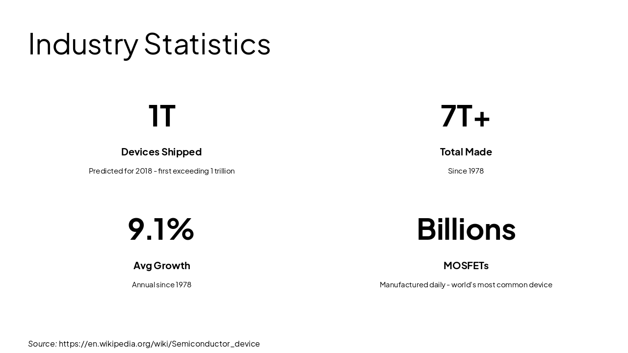
Source: https://en.wikipedia.org/wiki/Semiconductor_device
---
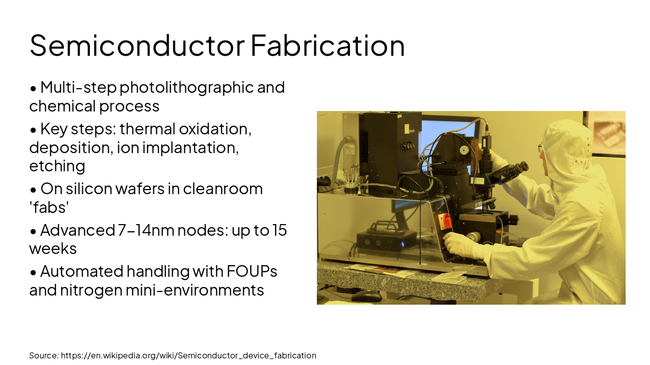
Source: https://en.wikipedia.org/wiki/Semiconductor_device_fabrication
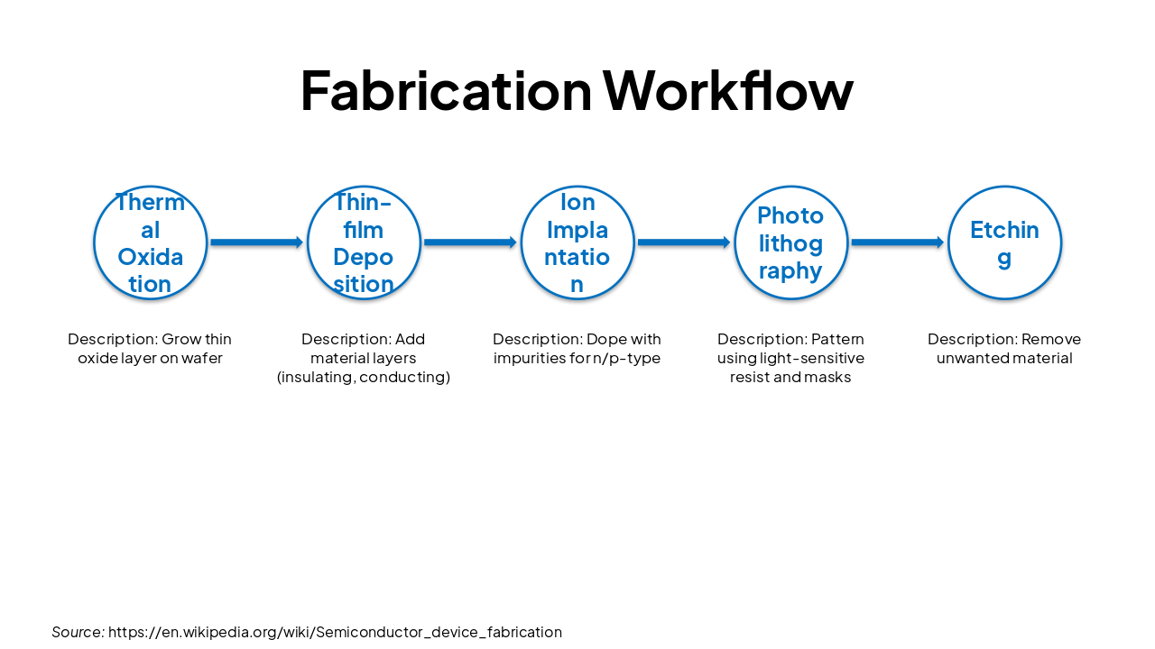
| Step | Description |
|---|---|
| Thermal Oxidation | Grow thin oxide layer on wafer |
| Thin-film Deposition | Add material layers (insulating, conducting) |
| Ion Implantation | Dope with impurities for n/p-type |
| Photolithography | Pattern using light-sensitive resist and masks |
| Etching | Remove unwanted material |
Source: https://en.wikipedia.org/wiki/Semiconductor_device_fabrication
Source: https://en.wikipedia.org/wiki/Semiconductor_device
Explore thousands of AI-generated presentations for inspiration
Generate professional presentations in seconds with Karaf's AI. Customize this presentation or start from scratch.
