Design and Analysis of 1.8V-to-1.2V LDO Regulator

Generated from prompt:

Create a PhD/Industry-level technical presentation titled "Design and Analysis of a 1.8V to 1.2V Low Dropout Regulator (LDO)". Specifications: - Input Voltage: 1.8V - Output Voltage: 1.2V - Maximum Load Current: 10mA - Output Capacitor: 3pF - With output capacitor (not capacitor-less) - No simulation slides - No layout/area slides Include ~30 professional slides with strong theoretical depth and equations. Slide Outline: 1. Title Slide 2. Problem Statement 3. Applications in SoCs and Mixed-Signal Systems 4. System-Level Specifications 5. LDO Architecture Overview 6. Detailed Block Diagram Amplifier Section: 7. Error Amplifier Requirements (Gain, BW, Offset) 8. Common Source Amplifier Analysis (Gain equation) 9. Differential Amplifier (CMRR, ICMR) 10. Folded Cascode Op-Amp Architecture 11. DC Gain Derivation 12. ICMR and OCMR Analysis 13. Input Offset Impact on Output Accuracy Pass Device Section: 14. Pass Transistor Operation Regions 15. PMOS vs NMOS Trade-offs (justify PMOS choice) 16. Pass Device Sizing for 10mA Load 17. Dropout Voltage Derivation Stability & Control: 18. Small-Signal Model of LDO 19. Loop Gain Derivation 20. Pole-Zero Locations 21. Phase Margin and Gain Margin Targets (>60°, >10dB) 22. Compensation Strategy with 3pF Output Capacitor Performance Metrics: 23. PSRR (Low-Frequency and High-Frequency Behavior) 24. Slew Rate (SR = I/C) 25. Transient Response and Settling Time (Ts) 26. Line Regulation (ΔVout/ΔVin) 27. Load Regulation (ΔVout/ΔIload) 28. Load Current Limitation and Power Dissipation Final Section: 29. Design Trade-offs (Area, Stability, Speed, PSRR) 30. Performance Summary Table 31. Conclusion Use a professional dark-theme style with clean equations and technical formatting suitable for PhD defense or industry review.

Technical review of a low-dropout regulator (LDO) design for low-voltage SoCs: from problem statement and specs to error amplifier, PMOS pass device, stability analysis, and performance metrics like PSRR >60dB, PM >60°, for Vin=1.8V, Vout=1.2V, Imax=

February 22, 202620 slides
Slide 1 of 20

Slide 1 - Design and Analysis of a 1.8V to 1.2V Low Dropout Regulator (LDO)

Design and Analysis of a 1.8V to 1.2V Low Dropout Regulator (LDO)

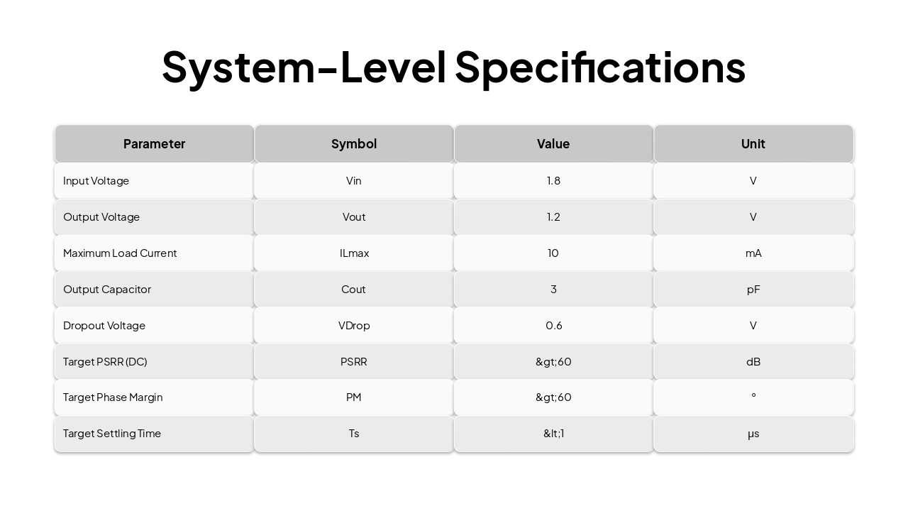
Vin = 1.8V, Vout = 1.2V, Imax = 10mA, Cout = 3pF PhD/Industry Technical Review

---

Photo by Umberto on Unsplash

Slide 1 - Design and Analysis of a 1.8V to 1.2V Low Dropout Regulator (LDO)
Slide 2 of 20

Slide 2 - Presentation Agenda

  • Problem Statement & Applications
  • System-Level Specifications
  • LDO Architecture Overview
  • Error Amplifier Section
  • Pass Device Section
  • Stability & Control
  • Performance Metrics
  • Design Trade-offs & Conclusion

---

Photo by Aron Visuals on Unsplash

Slide 2 - Presentation Agenda
Slide 3 of 20

Slide 3 - Section 1: Introduction

1

Problem Statement

Motivation for LDOs in Low-Voltage SoCs

---

Photo by MARIOLA GROBELSKA on Unsplash

Slide 3 - Section 1: Introduction
Slide 4 of 20

Slide 4 - Problem Statement

  • LDO enables regulation when Vin ≈ Vout (dropout = 0.6V here)
  • Advantages over switching regs:
  • • No switching noise
  • • Smaller size: no inductors/transformers
  • • Simpler design: reference + amplifier + pass element
  • Disadvantage: Power dissipation = (1.8-1.2V)×I_L = 6μW at 10mA

Source: Wikipedia: Low-dropout regulator

Slide 4 - Problem Statement
Slide 5 of 20

Slide 5 - Applications in SoCs & Mixed-Signal Systems

  • SoC Integration: Local regulation reduces off-chip passives
  • Mixed-Signal: Supplies clean Vout=1.2V to ADCs, DACs, PLLs
  • Low dropout ideal for stacked power domains (1.8V digital → 1.2V analog)
  • Battery-powered IoT: Efficient at low Vin-Vout differential
Slide 5 - Applications in SoCs & Mixed-Signal Systems
Slide 6 of 20

Slide 6 - System-Level Specifications

ParameterSymbolValueUnit
Input VoltageVin1.8V
Output VoltageVout1.2V
Maximum Load CurrentILmax10mA
Output CapacitorCout3pF
Dropout VoltageVDrop0.6V
Target PSRR (DC)PSRR>60dB
Target Phase MarginPM>60°
Target Settling TimeTs<1μs
Slide 6 - System-Level Specifications
Slide 7 of 20

Slide 7 - Architecture Overview

2

LDO Architecture Overview

Reference, Error Amplifier, Pass Device & Feedback

---

Photo by MARIOLA GROBELSKA on Unsplash

Slide 7 - Architecture Overview
Slide 8 of 20

Slide 8 - Detailed LDO Block Diagram

  • Bandgap reference generates Vref (e.g., 0.6V)
  • Error amplifier: Vout/2 → Vfb vs Vref
  • PMOS pass transistor Mp controls Iout
  • Feedback divider R1-R2 sets Vout=1.2V
  • Cout=3pF stabilizes dominant pole

---

Photo by Randall Bruder on Unsplash

Slide 8 - Detailed LDO Block Diagram
Slide 9 of 20

Slide 9 - Amplifier Section

3

Error Amplifier Design

Gain, Bandwidth, Offset, CMRR Requirements

---

Photo by MARIOLA GROBELSKA on Unsplash

Slide 9 - Amplifier Section
Slide 10 of 20

Slide 10 - Error Amplifier Requirements

  • DC Gain: A0 > 60 dB (Vout accuracy < 0.1%)
  • GBW > 10 MHz (transient response)
  • Input Offset: Vos < 1 mV
  • CMRR > 80 dB, PSRR > 60 dB (@DC)
  • Slew Rate SR > 1 V/μs
  • Low input bias current for R_feedback
Slide 10 - Error Amplifier Requirements
Slide 11 of 20

Slide 11 - Amplifier Architectures: CS vs Differential

Common Source Amplifier Gain: Av = -g{m1} (r{o2} || r{o4}) ~40 dB typical in 180nm High GBW but poor PSRR/CMRR Simple but insufficient for LDO

Differential Amplifier CMRR = 20 log{10} (Ad / Acm) ICMR: V{SS} + V{DSsat} to V{DD} - |V{GS}| - V{DSsat} High gain with current mirror load PSRR improves with matching

Slide 11 - Amplifier Architectures: CS vs Differential
Slide 12 of 20

Slide 12 - Folded Cascode Op-Amp Architecture

  • High DC gain: >80 dB
  • Improved ICMR for 1.8V supply
  • Single pole dominant response
  • Low power suitable for LDO
  • Compensation via output cap

---

Photo by Axel Richter on Unsplash

Slide 12 - Folded Cascode Op-Amp Architecture
Slide 13 of 20

Slide 13 - DC Gain Derivation - Folded Cascode

  • Input pair gain: A1 = g{m1} (r{o1} || r{o3})
  • Cascode gain: A2 = g{mc} (r{oc1} || r{oc2}) (1 + g{mc} r{oc2})
  • Total Av = A1 × A2 ≈ gm r_o ^2 > 80 dB (90 dB typ.)
  • High Rout enhances loop gain
Slide 13 - DC Gain Derivation - Folded Cascode
Slide 14 of 20

Slide 14 - ICMR, OCMR & Offset Analysis

  • ICMRmin = V{GS1} + V{DSsat,tail} + V{DSsat,fold}
  • ICMRmax = VDD - |V{GS,fold}| + V{DSsat}
  • OCMR: V{SS} + V{DSsat} to VDD - V{DSsat}
  • Offset impact: ΔVout ≈ V{os} / (1 + A0 β) < 1mV / 1000 = 1μV
Slide 14 - ICMR, OCMR & Offset Analysis
Slide 15 of 20

Slide 15 - Pass Device

4

Pass Transistor Design

PMOS vs NMOS Trade-offs & Sizing for 10mA

---

Photo by MARIOLA GROBELSKA on Unsplash

Slide 15 - Pass Device
Slide 16 of 20

Slide 16 - PMOS vs NMOS Pass Device Trade-offs

PMOS Pass Transistor (Chosen)

  • Low V{GS} sufficient (V{GS} = Vout - V{gate} ≈ 0.6V)
  • No bootstrap circuit needed
  • Good for dropout < V{TH}
  • Ron ∝ 1/(W/L μp Cox (V{GS}-V{TH}))

NMOS Pass Transistor

  • Higher mobility μn > μp → lower Ron
  • Requires V{GS} > Vin (bootstrap/driver needed)
  • Complex for low dropout
  • Poor for Vin ≈ Vout + small dropout
Slide 16 - PMOS vs NMOS Pass Device Trade-offs
Slide 17 of 20

Slide 17 - Pass Device Sizing & Dropout Derivation

  • Target Ron < V{drop}/I{Lmax} = 0.6V/10mA = 60 Ω
  • PMOS (W/L) ≈ μn Cox (V{GS}-V{TH}) Ron ^{-1} → W/L ≈ 200/0.18 μm
  • Dropout V{drop} = IL R{on} + I_Q (negligible)
  • Operation: Saturation (fast transient) → Triode (steady-state regulation)
  • Max Pdiss = 6 mW
Slide 17 - Pass Device Sizing & Dropout Derivation
Slide 18 of 20

Slide 18 - Stability Analysis

5

Stability & Control Loop

Small-Signal Model, Pole-Zero, Phase/Gain Margin

---

Photo by Claudio Guglieri on Unsplash

Slide 18 - Stability Analysis
Slide 19 of 20

Slide 19 - Small-Signal Model of LDO

  • Loop gain T(s) = A(s) β Rout / (Rout + 1/sCout)
  • Dominant pole fp1 ≈ 1/(2π Rout Cout)
  • Non-dominant poles from amp, pass device
  • Zero from ESR (negligible at 3pF)
  • Target PM >60°, GM >10dB

---

Photo by Ludovico Ceroseis on Unsplash

Slide 19 - Small-Signal Model of LDO
Slide 20 of 20

Slide 20 - Key Performance Metrics & Targets

MetricTargetEquation/Notes
PSRR (DC)>60 dBPSRR = 20 log (ΔVsupply / ΔVout)Slew Rate>1 V/μsSR = Itail / CcompSettling Time<1 μsTs = 4 / (GBW × ln(1/ε))Line Reg.<1 mV/VΔVout/ΔVinLoad Reg.<1 mV/mAΔVout/ΔIL × R_onPhase Margin>60°Stability criterionGain Margin>10 dB

Source: Wikipedia: Power supply rejection ratio

Slide 20 - Key Performance Metrics & Targets

Discover More Presentations

Explore thousands of AI-generated presentations for inspiration

Browse Presentations
Powered by AI

Create Your Own Presentation

Generate professional presentations in seconds with Karaf's AI. Customize this presentation or start from scratch.

Create New Presentation

Powered by Karaf.ai — AI-Powered Presentation Generator